GLF72112
3 A, Ultra-low Power IQSmartTM Load Switchwith True Reverse Current Blocking
Features
- Rise Time tR @ 3.3V 18µs
- True Reverse Current Blocking
- Ultra-Low IQ: 1.3 µA Typ @5.5 VIN
- Ultra-Low ISD: 24 nA Typ @5.5 VIN
- Low RON: 29 mΩ Typ @5.5VIN
- IOUT Max: 3 A
- Wide Input Range: 1.5 V to 5.5 V6 VABS max
- Controlled Rise Time
- Internal EN Pull-Down Resistor, REN
- 0.97 mm x 0.97 mm x 0.55 mm
Wafer Level Chip Scale Package
Applications
- Mobile Devices
- Wearables
- Low Power Subsystems
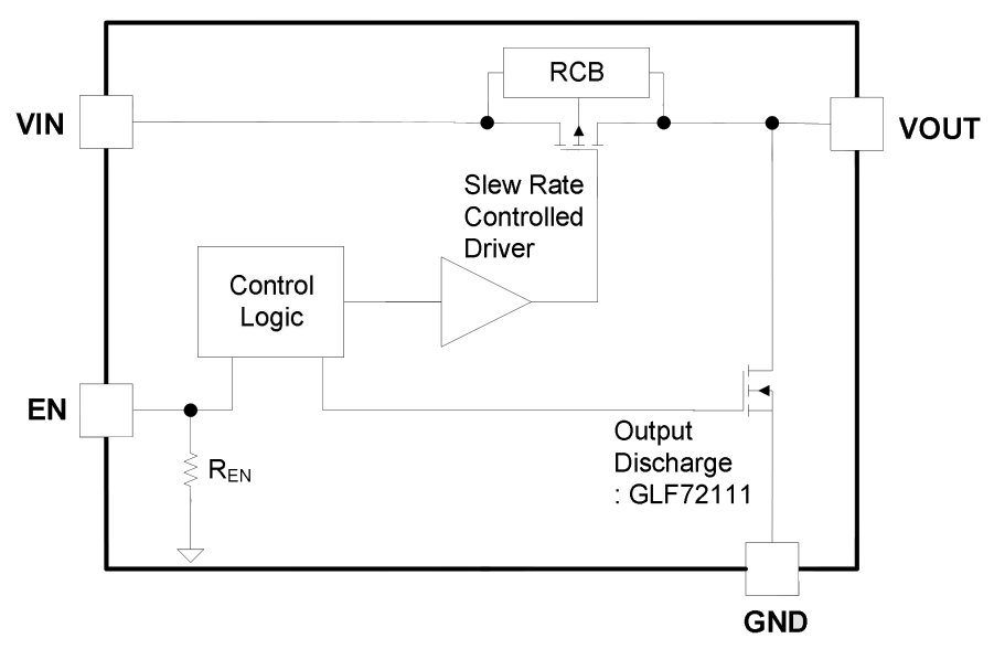
FUNCTIONAL BLOCK DIAGRAM
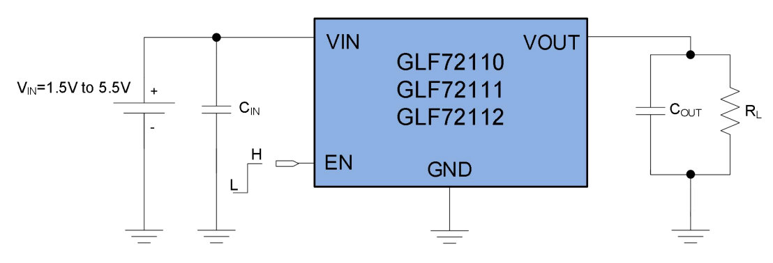
APPLICATION SCHEMATIC
PRODUCT DESCRIPTION
The GLF72110 / GLF72111 / GLF72112 is an advanced technology fully integrated IQSmartTM load switch device with True Reverse Current Blocking (TRCB) technology and slew rate control of the output voltage.
The GLF72110 / GLF72111 / GLF72112 offers industry leading True Reverse Current Blocking (TRCB) performance, featuring an ultra-low threshold voltage. It minimizes reverse current flow in the event that the VOUT pin voltage exceeds the VIN voltage.
The GLF72110 / GLF72111 / GLF72112 has industry leading efficiency. It features a RON as low as 29 m Ω typical at 5.5 V, reducing power loss during conduction. The device also features ultra-low shutdown current (ISD) to reduce power loss and battery drain in the off state. When EN is pulled low, and the output is grounded, the GLF72110 / GLF72111 / GLF72112 can achieve an ISD as low as 24 nA typical at 5.5 V.
The GLF72110 / GLF72111 / GLF72112 load switch device supports an industry leading wide input voltage range and helps to improve operating life and system robustness. Furthermore, one device can be used in multiple voltage rail applications which helps to simplify inventory management and reduces operating cost.
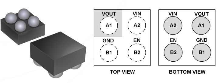
The GLF72110 / GLF72111 / GLF72112 load switch device is small, utilizing a chip scale package with 4 bumps in a 0.97 mm x 0.97 mm x 0.55 mm die size and a 0.5 mm pitch.
